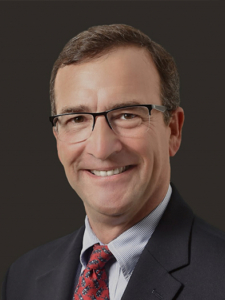
Keynote #1 – James A. O’Neill Senior VP and CTO of Entegris
Presentation Title: “Materials Challenges for the Semiconductor Industry”
Bio:
Jim has been Entegris’ senior VP and CTO since September 2015. He is responsible for the innovation process within the company including the development of new products and the global technology centers where Entegris collaborates with customers – the leading manufacturers of semiconductors – to solve their most complex technology challenges.
Jim joined Entegris in 2014 as part of the acquisition of ATMI, where he was senior VP of electronic materials. Prior to that, he worked at IBM for 23 years where he held several technical and leadership roles in semiconductor research, development, and manufacturing. In one of those assignments, Jim set up and ran IMB’s research operation at Albany Nanotech from 2007 to 2010 focused on the development of IBM’s 14nm node technology.
Jim earned a PhD in Physical Cheistry at Columbia University and a Bachelor of Science degree in Chemistry from Yale University. He holds 19 U.S. patents and has 46 technical publications.
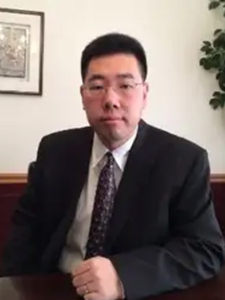
Keynote #2 – Huiming Bu Vice President, Global Semiconductor R&D and Albany Operations, IBM Research
Presentation Title: “Technology Innovations to Fuel 1T Transistors”
Bio:
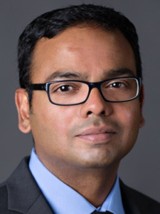
Keynote #3 – Dr. Nirmal Ramaswamy Vice President, Advanced DRAM and Emerging Memory Technology, Micron Technology Inc.
Presentation Title: “Memory Technology: Status and Scaling Perspective”
Bio:
Dr. Nirmal Ramaswamy is currently the Vice President of Advanced DRAM and Emerging Memory Technology at Micron Technology Inc. He has a bachelor’s degree in metallurgical engineering from Indian Institute of Technology, Madras, India, a PhD in Materials Science and Engineering from Arizona State University and is a graduate of the Stanford Graduate School of Business Executive Program.
Dr. Ramaswamy joined Micron in 2002 and has served in various leading roles in process development, process integration and technology development in DRAM, NAND, and Emerging Memories. He is currently responsible for 3D DRAM Technology, CMOS platforms for DRAM and Emerging memory Technology. He holds more than 250 issued patents in the field of semiconductors
Invited Speakers
Christoph Adelmann
imec
“Intermetallic Compounds as Alternatives to Copper for Advanced Interconnect Metallization”
Hsiao-Kang Chang
TSMC
“Airgap Integration on Patterned Metal Lines for Advanced Interconnect Performance Scaling”
Sascha Hermann
TU Chemnitz
“Stress-configurable 1D/2D nanodevices on waferlevel”
Woong Sun Lee
SK Hynix
“7 years after the A10 processor, the ERA of Heterogeneous Integration”
Byeong Sung Kim
Samsung Electronics
“Beyond Optical Scaling – Roles and Opportunities for DTCO in Angstrom-Scale Era”
Stéphane Moreau
CEA-LETI
“Recent advances on qualification and reliability of Cu/SiO2 to Cu/SiO2 hybrid bonds for 3D Integrated Circuits”
Stefan Müller
FMC
“BEOL-integrated ferroelectric RAM for advanced semiconductor technology nodes”
Jörg Schuster
Fraunhofer ENAS
“Towards knowledge enhanced process models for semiconductor fabrication”
Seung-Chul Song
Google
“A Holistic Approach to System Design Technology Co-Optimization for Deep Single Digit Nodes”
Kirill Monakhov
Leibniz Institute of Surface Engineering (IOM)
“Solution-processable molecular oxides for integrated memories”
André Clausner
Fraunhofer IKTS
Mechanical BEoL Robustness Evaluation Using Variable Loading Strategies and Acoustic Emission Damage Monitoring


